Lee Jae-yong plans to invest 20 trillion won in R&D sector
Lee Jae-yong plans to invest 20 trillion won in R&D sector
Posted August. 20, 2022 07:34,
Updated August. 20, 2022 07:34

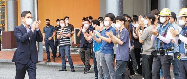
Vice Chairman of Samsung Electronics Lee Jae-yong presented a mid- and long-term vision for the technological development of semiconductors over the next generations at a groundbreaking ceremony for a semiconductor R&D complex on the company’s Giheung campus located in Yongin, Gyeonggi Province, on Friday afternoon as part of his first steps taken as the company’s leader since he returned to business. “Samsung begins a new journey on the Giheung campus where it took the very first step to build semiconductor manufacturing facilities 40 years ago,” Lee said.
Samsung heir made his first official appearance on a business-related occasion since he received a special pardon on Liberation Day, just four days ago. MLee emphasized that aggressive investments in R&D projects for the next generation and beyond have upgraded Samsung’s semiconductors as we know it today, asking employees to hold the tradition of putting technology-centric and preemptive investments first and build the future based on technologies that no one has ever seen before.
The Giheung campus was built up as Samsung Electronics’ first semiconductor facilities in 1983. The company announced on Friday that a total of 20 trillion won will be invested by 2028 in the R&D complex on the campus to turn it into a hub equipped with cutting-edge technologies in all semiconductor fields from memory through system semiconductors to foundries. “The birthplace of Samsung’s semiconductors will become a new beginning of the future,” said a Samsung executive.
His decision to visit the Giheung campus right after his return implies how he views the global semiconductor industry. Indeed, as major countries including South Korea have recently given economic and security priority to semiconductors, not only businesses but also governments are scrambling to invest in technological development. After Friday’s groundbreaking ceremony, he moved to the Hwaseong campus in the province to join a round-table meeting with executives and employees for the first time in two years. Given that he can return to the forefronts of business following the Aug. 15 special pardon, a series of his activities seemingly intended to catch up with employees internally and get the organization aligned.
Do-Young Kwak now@donga.com


